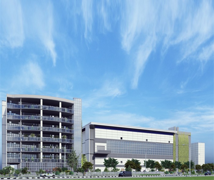
Semiconductor Fab Master Planning
Setting up a semiconductor FAB is very challenging for the semiconductor firms.
Challenges:
Finding a space, Green field land or existing Building.
Comply to JTC Planning Submission Fact Sheet.
Unsure of total project cost and duration of project.

Our Solution
Provide 30% Concept Design with estimated cost.
Firm up the cleanroom layout, Sub FAB, Level 1, Space Planning for CUB Building (Cooling Tower, Chilled Water Plant, Clean room MAU Room), Admin building, Warehouse , Electrical substation, space for On Site N2 Generator Plant and BSGS Yard.
Obtain approval from JTC.
Firm up the CSA Design and estimate the CSA Cost.
Provide all the Utilities equipment sizing and Block Diagram and estimate the MEP Cost.